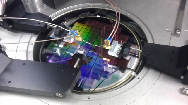
Branded as the “wonder material”, the researchers have been able to use graphene in creating the most advanced integrated circuit. This has the potential to allow mobile devices to transmit data far quicker.
Graphene was first created in 2004 and since then has been subject to a lot of study. Made up of just a single layer of carbon atoms, the aim is to harness its incredible electrical, thermal, optical and mechanical properties. These make it more energy efficient and cheaper compared to silicon.

According to IBM, graphene is well suited for wireless communications. Now that we see more big data applications, it has become more important to improve mobile devices so that they can transmit and receive large amounts of data, more efficiently.
“This is the first time that someone has shown graphene devices and circuits to perform modern wireless communication functions comparable to silicon technology,” said Supratik Guha, director of physical sciences at IBM Research.
Graphene has nano-scale dimensions, making it difficult to incorporate in to a circuit because it can be easily damaged. However, scientists have developed a manufacturing method that can preserve the quality of the graphene transistor, making it the most sophisticated graphene-based integrated circuit.
This breakthrough is considered to be a step towards true graphene technology.
[Image via Flickr]
SOURCE: http://www.bbc.co.uk/news/science-environment-25944824
No comments:
Post a Comment